Enhanced Photo-response of MoS2 Photodetectors by a Laterally Aligned SiO2 Nanoribbon Array Substrate
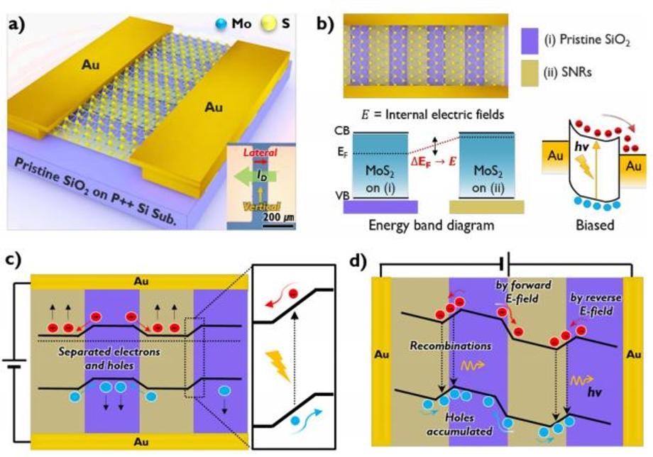
Achieving both high photocurrent and small dark current is necessarily required for the enhanced performance of molybdenum disulfide (MoS2) photodetector (PD). In the twodimensional transition metal dichalcogenide PD, inevitable recombinations occur highly at intrinsic defects of MoS2and impede photo-generated carrier releasement into electrodes, resulting in a poor PD performance. To address this issue without introducing a superiorly highcrystalline MoS2 monolayer and/or complex PD architecture, we for the first time report a facile method of simply transferring the MoS2 onto a periodically aligned silicon dioxide nanoribbons (SNR) array substrate fabricated by 325 nm laser interference lithography. Interestingly, two different n-doping states are arranged alternately on the MoS2 layer, depending on the underlying region of contact substrate (pristine SiO2 and SNR). The different n-doping levels induce internal electric fields by which photo-generated carriers are separated, reducing the recombination chance. The MoS2 PD on the SNR array substrate shows an improved photocurrent to dark current ratio of ~360 (~7 times larger than that of the reference PD on the pristine SiO2 substrate), while producing a small dark current of ~10-12 A at VG = 0 V. Our method paves the way for enhancing the performance of other 2D materials-based optoelectronic devices.